
.png)
ERS electronic Unveils Fully Automated 310 x 310 mm Panel-Level Packaging System to Power AI and Chiplet Architectures

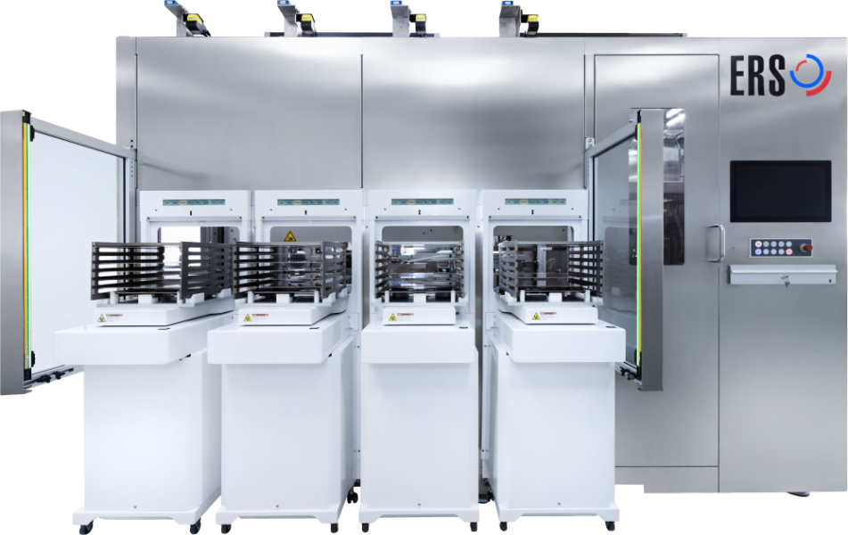
ERS electronic, the industry leader of thermal management solutions for semiconductor manufacturing, today announced its fully automated panel-level packaging (PLP) system for 310×310 mm substrates.
The machine integrates temporary carrier bonding, debonding, and detaping into a single automated platform at 13 panels per hour, eliminating inter-tool transfers across three thermally critical process steps. The first unit has been delivered to a leading semiconductor manufacturer for integration into its panel production line.
The machine is developed and manufactured at the company’s Advanced Packaging facility in Barbing, Germany. The facility combines ERS's 55 years of thermal management expertise with more than 30 years of in-house machine-building capability, following ERS's 2024 integration of a semiconductor specialist equipment engineering team.
ERS is considered an early adopter of panel-level packaging, as it shipped its first commercial panel-level tool to Fraunhofer IZM in Berlin in 2018. The 310×310 mm panel format is gaining traction across the industry because it improves substrate area utilisation significantly compared to 300 mm circular wafers.
The panel-level packaging segment is projected to grow at a compound annual growth rate of over 40% over the next five years, according to Yole Group1. As dual-carrier bonding and debonding workflows become increasingly important for backside processing in 3D IC, HBM and 2.5D IC packaging, ERS's integrated platform addresses these requirements in a single automated system.
In dual-carrier processes, bonding and debonding typically requires separate machines, often located at different points on the fab floor. Moving panels between them introduces handling steps, transit time, and the risk of substrate damage. ERS’s machine consolidates all three process steps within one platform, so panels move between process modules rather than between machines, thereby reducing handling time and risk without changes to the surrounding fab layout.
"Our new machine reflects our commitment to solving real manufacturing challenges. By integrating three process steps that have traditionally required separate tools into one automated platform, we're enabling customers to streamline production, improve process consistency, and achieve higher yield and throughput,” says Laurent Giai-Miniet, CEO of ERS electronic GmbH.
About ERS:
ERS electronic GmbH, based in the Munich suburb of Germering, has been providing innovative thermal management solutions to the semiconductor industry for more than 50 years. The company has gained an outstanding reputation, notably with its fast and accurate air cooling-based thermal chuck systems for wafer probing. In 2008, ERS extended its expertise to the Advanced Packaging market. Today, their fully automatic and manual debonding and warpage correction systems can be found on the production floors of most semiconductor manufacturers and OSATs worldwide.
Copyright 2026 GlobeNewswire, Inc.
Berita Lainnya
OTC Markets Group Appoints JP Chan to Lead Asia-Pacific Growth in Hong Kong
Crypto Wealth Holds Up in 2026 as Bitcoin Retreats from Record Highs
Mavenir First Major Network Software Vendor to Receive 5G Packet Core Network Function Certification Under Germany's BSI NESAS Scheme
Urban-Gro Positioned to Capture Growth as T20 Cricket Franchise Valuations Exceed $1.6 Billion and Global Media Expansion Accelerates
From the Team Behind 'PRIMITIVE WAR' Comes a New Cinematic Series: 'DINOSAURS OF THE WILD WEST'
Bitget Expands Agent Hub Ecosystem Through MuleRun Partnership to Advance Agentic Trading
Curia Memperluas Kapasitas Manufaktur Glasgow dan Meningkatkan Platform Pengembangan Lini Sel
Cambodia Receives Institutional Capability Development Plan to Strengthen NPCC and Advance Productivity-led Growth
nCino Announces Nick Edwards as Managing Director for APAC
Freshworks Appoints Ryan Manning as Chief Product and Technology Officer
Q2 Metals Announces Inferred Mineral Resource Estimate on the Cisco Lithium Project with 295 Million Tonnes Grading 1.36% Li2O
Teva to Host Conference Call to Discuss Third Quarter 2026 Financial Results on November 3, 2026 at 8 a.m. ET